Applied and Integrated Photonics

We use our expertise to design and manufacture micro-optical elements, including equipment for their fabrication.
Integration of micro-optics, photonic optics, and bulk optics into scientific instruments opens new possibilities for the development of new classes of systems to broaden our understanding of matter interaction and allows for complex investigation of biological and chemical processes, as well as the miniaturization of these instruments.
Currently, our team focuses on the development of advanced imaging and hyperspectral imaging systems using specially designed optical elements. These are widely applicable in plant agriculture and microbiology.
In addition, we are developing an image processing software for analyses of morphological composition at a sub-micrometer scale. We process large datasets acquired using our instruments using machine learning algorithms.
R&D profile of our group

- Compact optical tweezers system with MEMS steering optics and optomechanics for biomedical applications.
- The use of photolithographic methods, wet and dry etching to produce optical elements, microfluidics and metasurfaces.
- Microchip for optical trapping of micro-objects under low pressure.
- Metaoptics structures for aberration-free imaging and spectroscopy systems.
- Inspection by Scanning Probe Microscopy with emphasis on the surface topography of prepared nanostructures and films & coatings.
- Determination of mechanical properties such as elastic modulus, hardness or film adhesion by nanoindentation measurements and scratch testing.
- Microfluidic acoustic wave based sorting chips.
- Arbitrary shaped optical gratings and micro-optical elements.
NEW TECHNOLOGIES IN HYPERSPECTRAL IMAGING
Design of photonic elements and integration of photonic elements into innovative imaging and spectroscopic optical systems.
We develop highly integrated photonic elements based on micro-optics and meta-optics for light transformation in the optical systems of imaging systems, classical and imaging spectrometers, and special photonic chips for studying the mechanical behavior of micro-objects in strongly focused light fields.
- Development of imaging spectrographs with submicron spectral resolution.
- Development of snapshot imaging spectrographs.
- Design of MEMS based spectrographic systems.
- Software development based on machine learning and artificial intelligence that allow fast spatial and spectral recognition of objects.
- Hyperspectral imaging is useful for inline sorting and quality control.
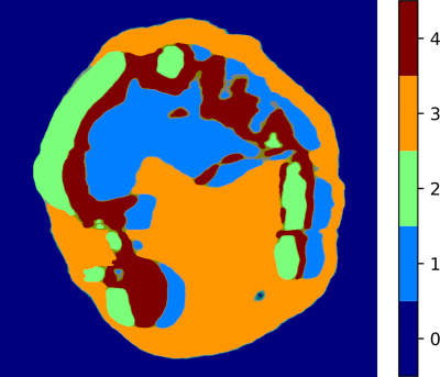
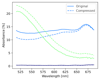
Hyperspectral recording of the internal structure of the alga Trachydiscus minutus and processing of spectra into individual classes using artificial intelligence methods.
 |
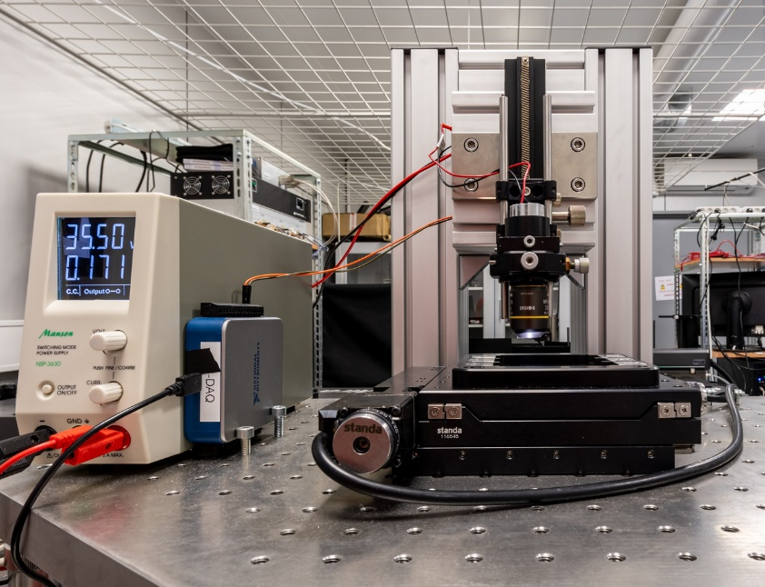 |
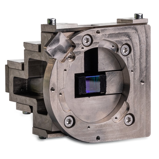
| Optomechanics for multispectral camera. | Hyperspectral microscope. |
SINGLE AND TWO-PHOTON LITHOGRAPHY
Development of a robust technology for the production of photonic elements.
Development of specialized devices and technology for recording high details (100 nm and less) with subsequent copying of the matrix to the substrate by deep reactive ion etching technology. We are intensively developing technologies for maskless recording of micro-optical elements with a two-photon stereolithography of our own design and fs laser-assisted reactive ion etching.
- Single photon large volume lithography system with a digitally addressable projection system for biological and material applications.
- High accuracy positioning of sample stage and objective using an interferometric closed loop.
- Precision two-photon lithography system with acoustooptics laser beam steering system for very fast and accurate microstructures writing.
- Development of writing strategies and special techniques for high-volume, high-resolution printing.
- Interference and holographic recording of microstructures using modulators and DLP technology.
- Beam shaping of writing beam by spatial modulators.
- Refraction and diffraction optics design and manufacturing.
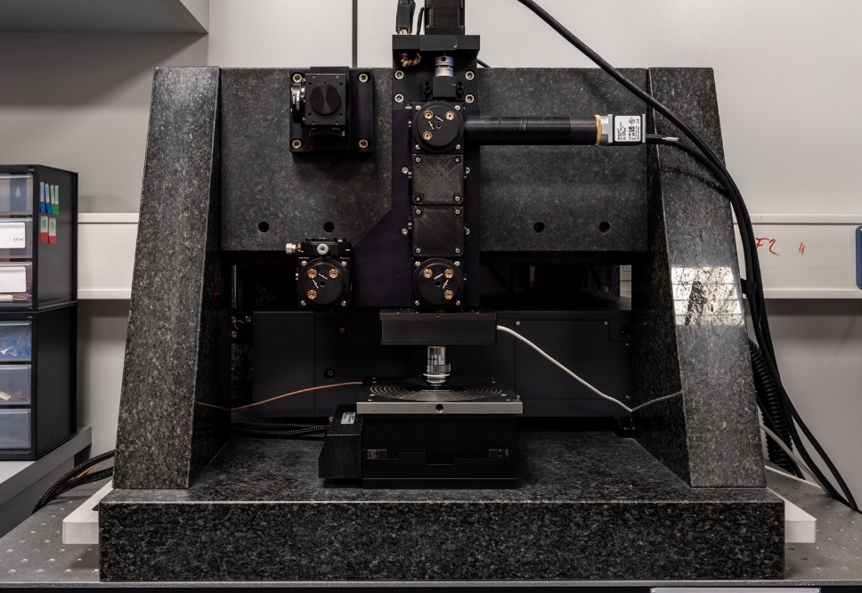
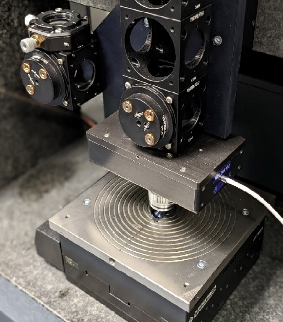
Two-photon stereolithograph.
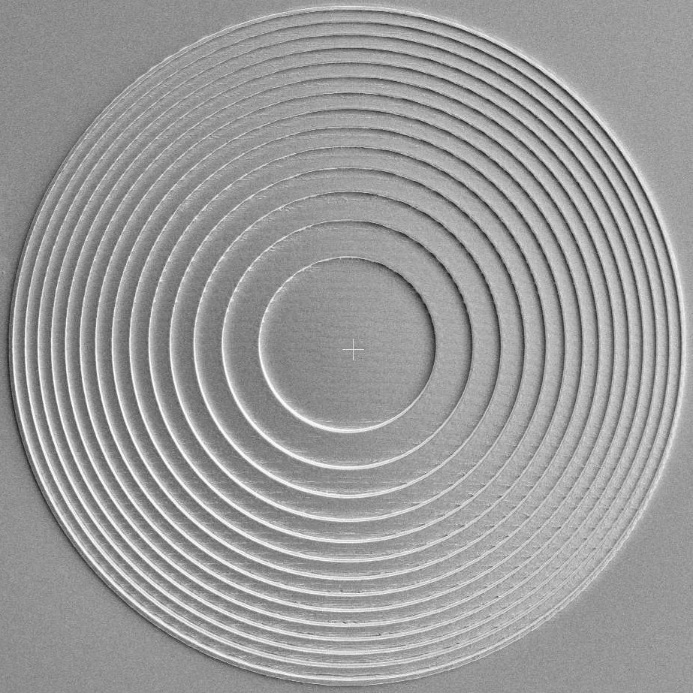
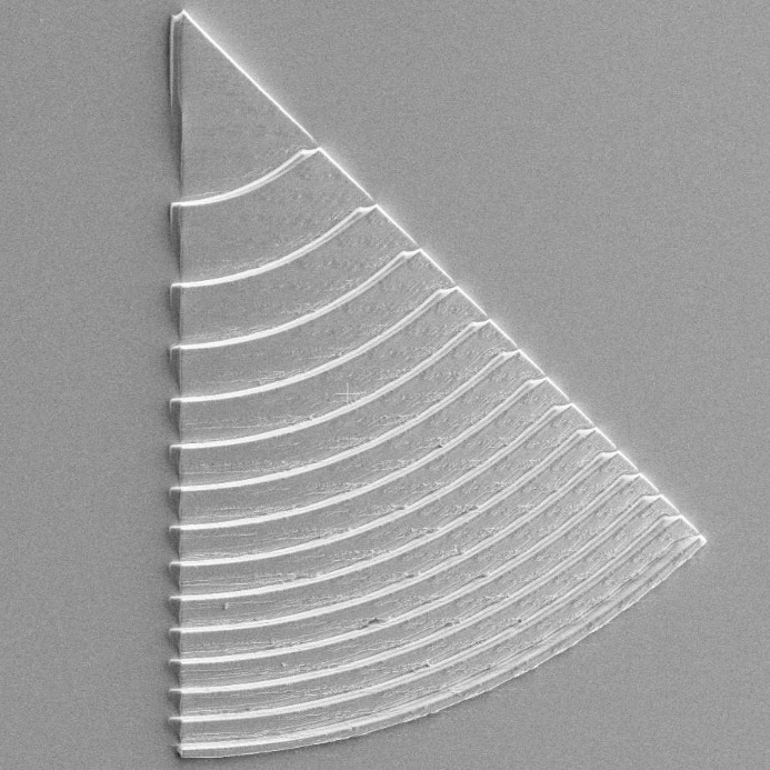
A Fresnel lens composed of concentric circular rings.
| Contacts | ||
| Ing. Mojmír Šerý, Ph.D. | sery@isibrno.cz | +420 541 514 535 |
| Ing. Tomáš Plichta, Ph.D. | plichta@isibrno.cz | +420 541 514 534 |
| Ing. Tadeáš Maňka, Ph.D. | manka@isibrno.cz | +420 541 514 534 |
| Ing. Petr Jedlička, Ph.D. | jedla@isibrno.cz | +420 541 514 524 |
| Ing. Lukáš Šilhan | silhan@isibrno.cz | +420 541 514 531 |
| Ing. Denisa Šilhanová | skrabalova@isibrno.cz | +420 541 514 531 |
| Mgr. Ondřej Vaculík | vacuon@isibrno.cz | +420 541 514 533 |
| Ing. Alžběta Gjevik | bety@isibrno.cz | +420 541 514 533 |
| Ing. Jakub Vejrosta | vejrys@isibrno.cz | +420 541 514 534 |
| Ing. Veronika Richterová | verich@isibrno.cz | +420 541 514 533 |
| Ing. Lukáš Kaleta | kaleta@isibrno.cz | +420 541 514 534 |
| Ing. Markéta Khýrová | khyrova@isibrno.cz | +420 541 514 534 |
| Tomáš Šilhan | tsilhan@isibrno.cz | +420 541 514 524 |


