


High resolution scanning electronmicroscopywith analytic techniques
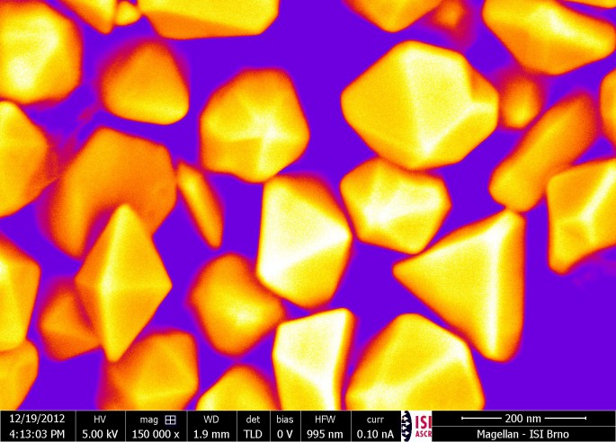
The high resolution scanning electronmicroscopy applications are met in nearly all scientific branches. In combinationwith the X-raymicroanalysis, EBSD and cathodoluminescence it provides information about the surface topography of a sample, its crystalografic orientation and its local quantitative chemical composition.
Scanning electron microscopes:
- FEI MAGELLAN 400
- JEOL JSM 6700F
- TESCAN VEGA 5130
Analysers:
- Energy dispersive analyzer of X-rays (INCA 350 and EDAX Apolo X)
- Electron Back Scattered Diff raction Analyzer (Hikari)
- Cathodoluminescence detector (Gatan MonoCL)
Advantages and application examples:
- Imaging with detectors of both transmitted and scattered signal provides complex information about the sample.
- Surface is observed at very low energies down to about 1 eV at high resolution.
- Secondary electrons informing about the surface topography are detected with two complementary detectors.
- Backscattered electrons are also detected with various detectors, with a possibility of acquiring the complete emission including the high angle scattered electrons not available in conventional instruments.
- Transmitted electrons are detected with segmented STEM detector, imaging in bright field (BF), dark field (DF) and high angle annular dark field (HAADF). The detector has high collection efficiency in wide range of primary beam energies from tens eV to 30 keV.
- Sub-nanometer resolution, achieved without any aberration corrector.
- Filter of secondary electrons is used to suppress charging effect in the image.
- Quantitative chemical composition (Apolo X or Inca energy) in combinationwith the high resolution imaging leaves very little unknown about any sample.
- EBSD detector (Hikari) is used for crystal orientation mapping, defect studies, phase and grain boundary identification in many materials.
- Cathodoluminescence detector (Mono CL 4) detects all light signal (ultraviolet, visible and infrared range) emitted from minerals, biological specimens, semiconductors and also limited volume specimens like nanofibres, thin films and nanoparticles. Emission spectra are taken with high spatial resolution.
