


Microlithography Techniques
|
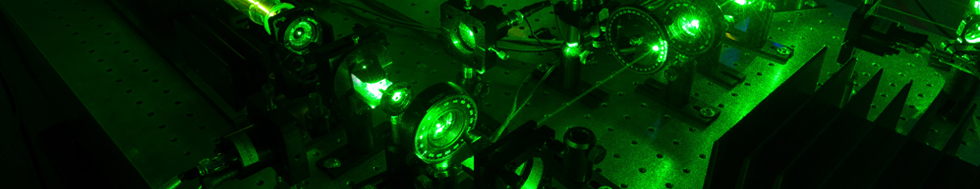
Technology of structures prepared in thin layers of metal and dielectrics on silicon or glass substrates. Combined electron beam lithography. Etching techniques: wet etching, plasma etching, reactive ion etching (RIE). Scattering of the electrons with a condensed matter during the electron beam exposure. Imaging techniques: optical microscopy, profilometry, confocal microscopy (CLSM), AFM, SEM. |
|
|
|
 |
The structure prepared by the anisotropic etching of silicon (calibration specimen for SEM — Scanning Electron Microscopy). |
|
E-Beam Lithography Group (EBL) Research Areas:
Offered Technologies: |
 |
Amplitude–phase mask for optical vortex beam. Wet etching of chromium; planar relief structure in PMMA resist. |
|
|
 |
The sandwich nano–structure prepared by RIE technique (Reactive Ion Etching) for the growth of carbon nano-cathodes. |
|
|
 |
|
||
| Processes for the prepariation of nanostructured Si3N4 membranes on silicon wafer; it comprises a series of lithographic and etching operations. |
|
||
 |
|
||
| Process for the combined exposure using two pattern generators of different energies. The development of the exposed resist may be done either by the method of independent resist development or by the method of simultaneous resist development. | |||
Výzkumná skupina:
Electron Beam Lithography