


E-Beam Lithography Technology
|
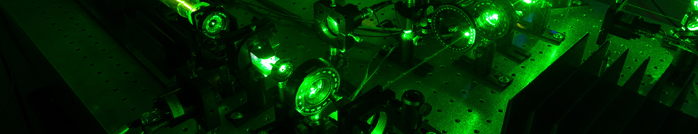
The group of Electron Beam Lithography (EBL) within the Special technology department developed the E-beam lithography technology and Optical diffractive structures.
|
|||
|
Dimension calibration samples.
|
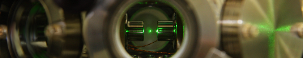
A required image is enregistered into the thin polymer layer (positive or negative electron resist) by the beam of electrons. The resist-layer mask is created by the development of the exposed patterns. The substrate surface (or the working layer previously deposited on the substrate – either a metallic or a dielectric one) is modified through the resist openings.
Selected R&D result used by industrial partners:
|
The group of Electron Beam Lithography Research areas:
Offered technologies: |
|


 Target 1951 USAF.
 Photomask for dynamic measurements of gravity.